Saturday, 11 April 2026

My Project Workflow

Projects can take a long time to bring to fruition. This means that I often have several on the go at the same time, which in turn can cause me to miss out some important steps. So I thought I'd gather all of the tips and tricks I've learned in one place as a reference.

The idea
  • scratch an itch
  • read other makers (for example on hackaday)
  • that new-fangled youtube can be useful too
Prototype
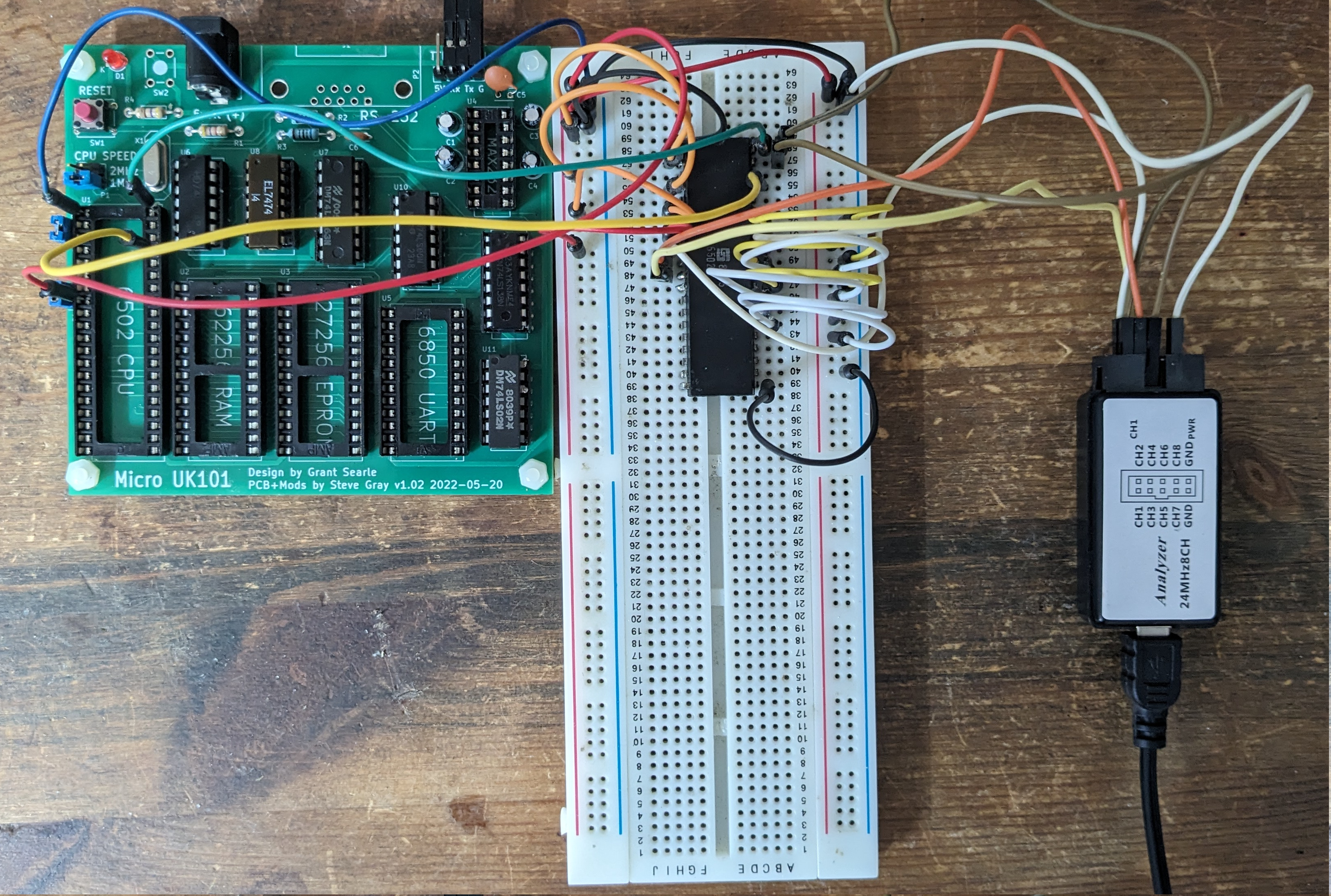
  • use a breadboard and dupont connectors for speed
  • sketch the schematic on paper as you go
  • use an llm for advice or as a search engine to find similar projects
  • plagiarise other people's designs, you might find one which does everything you need
Schematic
  • break out KiCad or similar and copy the paper schematic
  • separate subsystems and connect with labels
  • add test points (and expansion points if that makes sense)
  • use the electrical rules checker
  • rebuild the schematic on breadboard to test it
PCB Design
  • add component footprints
  • use the design rules checker
  • print the PCB at 1:1 on paper and check footprints
  • make holes in the paper with a pin and check footprints again!
  • use a ground plane and mounting holes
  • use the silk-screen for component values, labels and version information
  • add your email address (you never know)
  • use a plugin to send your design for fabrication (for example to PCBWay)
  • save the design and its firmware in version control (for example GitHub)
Board Assembly
  • don't rush!
  • add low-profile components first
  • socket everything you might want to reuse
  • solder up each subsystem and test immediately
  • clean off flux with isopropyl alcohol and a toothbrush
Post Mortem
  • if it works, document it on a blog like this one
  • if it doesn't, fix it immediately, update the version, and document it on a blog like this one
  • don't worry about anyone caring about your successes or failures!


Friday, 10 April 2026

Emulating a Commodore Chessmate

 A couple of years ago, Hackaday published a short piece on the Commodore Chessmate. As is usual with their articles, its shortness of length was more than made up by the breadth of its links. The last of these led to Hans Otten's Retro Computing page. 

(One of the few comments beneath the article is by Peter Jennings, creator of the original Microchess program, linking to his reminiscences about the Chessmate: well worth a read!)

Chessmate by Commodore

Anyway the article caught my attention because I'd had one of these as a nerdy kid. I remember opening it up, hoping to find... I don't know what, maybe a sort of PET? but not recognising many of the components; nowadays I could just Google it, and probably end up at Hans's page.

Among a wealth of other information, Hans provides ROM dumps and a memory map. I thought, should be pretty easy to write an emulation of that, and so it was. (The hardest part was probably mapping the 7-segment LEDs onto the TFT screen, which is to say: not very. Probably about a weekend in all.)

Chessmate by me

(The emulation uses r65emu, my emulator library for Arduino, running on an esp8266 connected to a TFT screen.)

Time passed and r65emu slowly improved. One update was to support other kinds of displays and keyboards besides the original TFT and PS/2. Sometime after this I decided to build a retro-modern version of the Chessmate with an anachronous mix of whatever parts I had lying around, and knocked it together on a couple of breadboards. 

I don't have a picture of that, but it was an unholy mess of wires, and languished on the side of my desk for over a year before I sat down with KiCad to turn it into something more permanent. I must have been in a rush because I made several mistakes with that PCB, getting some footprints wrong. I fixed them and parked the design, slightly depressed.

Things might have stayed like that for yet another couple of years, had I not been contacted out-of-the-blue by Liam from PCBWay who expressed interest in sponsoring r65emu. And so...
Chessmate by me and PCBWay

This uses a node32s microcontroller, push-button switches, a buzzer and 7-segment LED displays. The four status LEDs are represented by decimal points. Its software and hardware lives on GitHub.

It would be interesting to run a modern chess program on this hardware; one possible candidate is by Sergey Urusov.

(Incidentally, Michael Gardi has a much nicer modern rebuild of the Chessmate, complete with 3D-printed replica case!)


Monday, 19 January 2026

Scoping out a UK101

The first thing to measure when repairing a retrocomputer is the main oscillator. In a UK101, this is called CLK and found on U58 pin 3.

CLK (8MHz)

 This is divided by U29 and sent to the processor from pin 11 as Phi0 and reaches the counting chains as C0.

Phi0 (1Mhz)

The processor uses Phi0 to produce the processor clock Phi2. This is sent from U8 pin 39 to the hardware devices which populate the address and data buses.

Phi2 (1Mhz)

The counting chain is made up of U59, U60, U61 and U30. These divide C0 into C1-C15. About halfway along the chain are C8-C10, which are fed into the character generator's address lines A0-A2.

C8 (7.8kHz)

Ultimately this produces a Composite Video signal on J2 pin 12.

Video (15.5kHz)

So it's fairly certain that when this is connected to a monitor, there will be some sort of picture!

(This work also turned up an error in the serial clock generation. C3 (125kHz) is used to produce the transmit  clock TxCLK. However while the former is OK, the latter is missing: further investigation is required.)


Tuesday, 6 January 2026

Solving a simpler problem

Project Euler is a popular site among enthusiasts of mathematics and programming problems. A very common template for its problems goes something like:

Let F(n) be some function expressed in words. You are given that F(100) is some relatively small number. Find F(10^7).

 Often the best approach to such problems is to write a brute-force solution which gets the correct answer for the given data to verify that you understand the problem. Then examine the order of growth of this brute-force solution, say O(n^2), to determine what the best approach is, maybe O(n*log(n)), given that Project Euler says that all of its problems are solvable in under a minute.

This approach works well for software because it's easy to code up a brute-force solution and play around with it. It's not so useful for hardware for a similar reason: it isn't so easy to build hardware prototypes.

Nevertheless the MicroUK101 described last time was an attempt at a test-bed for those chips in the UK101 which weren't testable with Arduinos: the 6502 CPU and 6850 ACIA. A working MicroUK101 would verify that those chips were working too.

Unfortunately when assembled, it didn't work! Now what? Last time I tried to strip it back to the bare essentials required to test a 6502: a power supply, reset circuit and CPU clock. When this didn't work as expected, I had assumed that the 6502 had gone bad. This assumption was incorrect.

Time passed and recently I bought an OWON vds1022i USB oscilloscope and decided that an easy first task would be to fix the MicroUK101. Very quickly I discovered that the clock circuit wasn't oscillating at 4MHz as it ought to: according to the scope it was oscillating at 40MHz!

The simpler problem required another simpler problem: build the clock circuit on a bread-board and try to make it work there before making any changes to the PCB version. The problem turned out to be the 680R resistors in the clock oscillator: these did not provide the stability required, at least with the choice of crystal and 74LS04 I had on hand. Upping the resistors to 4k7 fixed the issue and with it the MicroUK101.

MicroUK101 by Grant Searle and Steve Gray

Incidentally if I were making changes to Steve Gray's PCB, I would drop the power switch and RS-232 interface, using only an FTDI adaptor to power the board and talk to it.

Friday, 14 June 2024

Testing a 6502 CPU

 It's relatively easy to test the UK101's discrete TTL chips using a simple Arduino-based IC Tester, and the ROMs can be read by an EPROM programmer but what to do about the more esoteric chips, i.e., the CPU and ACIA?

As CPUs go, the 6502 is a masterpiece of simplicity. It turns out that you can have it run the most basic of programs with no support logic whatsoever! This is the well-known NOP test, in which the CPU is fed an endless stream of No-Operation instructions, see for example here.


Breadboard 6502 flanked by Clock Circuit (L) and Logic Analyzer (R)

The image shows the test-set-up. The board on the left is a Micro UK101 which is only used as a power-supply, reset switch and clock source. (This is a more rewarding way of testing CPU and ACIA, but only if they both work!)

The CPU does not need many connections to run the NOP test: its data-bus is hard-wired to EA (the opcode for NOP), it also has IRQ and NMI tied high, and the input clock and reset line from the Micro UK101.
 
The logic analyser on the right is a cheap 8-channel model which works with PulseView. It is triggered by the reset pin (high-to-low transition) and samples A0, A1, A2 and the output clock.

When powered up and reset, the 6502 reads its reset vector at $FFFC and $FFFD. Unsurprisingly it reads the address $EAEA and jumps there. It then reads an endless stream of NOPs at every address between $0000 and $FFFF. Its address pins will show this.

Or they would show this, if the CPU was working. The screenshot below shows what happens most of the time:

Dead

The top trace is the reset line and the bottom one is the output clock, which seems to be working. The three lines in the middle are A0, A1 and A2 with nada.

However sometimes the CPU shows signs of life. About every 10 resets, there would be a short burst of activity for a few microseconds:
Some signs of life

So it looks as if this CPU is a goner. It was made by Synertek in the 35th week of 1980 and spent the last 40-odd years in a cold damp attic, where it expired: RIP.

Update: Hans Otten has written about NOP testers here.
Update #2: It seems my test-setup above was flakey and the CPU is actually OK: stay tuned!


Thursday, 14 March 2024

TommyPROM

Some time ago, I mentioned that I had been unable to test the various ROMs in the UK101, lacking an EPROM programmer. That has now been rectified, thanks to the fine work of Tom Nisbet, creator of TommyPROM

In addition to an Arduino sketch, the Github linked above hosts a couple of circuit boards, and I had them made as part of my last order from Seeed Studio.

TommyPROM with a very old 2716 EPROM

Populating this PCB cost under €10, quite the bargain. This version of the programmer can read 27-series EPROMs but can't manage the voltages required to program them.

Configuring the programmer requires editing the Arduino sketch for chip series and type, and uploading the modified sketch. This wouldn't pass muster in a commercial product but is absolutely fine for this project's target market: hobbyists on a budget.

Opening a serial port to the board shows the following menu:

Main Menu

Reading that EPROM, which is nearly 40 years old, produced the following output:

Amnesia?

Unsurprisingly, given its age, it seems to have lost its memory! Luckily it is not too difficult to find copies of UK101 (and Superboard) firmware online, Mark's Lab has copies for instance.

Burning old-school 27-series EPROMs requires more advanced hardware, and the second TommyPROM board I had made can do it, TommyPROM32. I will review that iteration when I have assembled it.

What the current version of TommyPROM can do is write to 28-series EEPROMs, e.g., an AT28C16. This is pin-compatible with the 2716 so once it arrives and has been programmed, the next step in testing the UK101 can be taken: hooking the board up to a logic analyser and spying on the data bus using another fine Open Source tool: 6502Decoder.

(I have several PCBs left over from that order. If you want one at cost, PM me.)

Update (April 2024): after some further investigation, it turns out that the basic TommyPROM can only handle 28-pin chips so any data retrieved from smaller chips (as above) won't be valid. TommyPROM32 is definitely the way to go here. Stay tuned for a review of that coming soon!


Sunday, 21 January 2024

Bodge Wiring

A bodge wire is defined as a "wire added to a PCB to fix errors in the layout or broken traces." The first is as a result of a design fault while the second arises from mistakes made in maintenance of an existing PCB.

Bodge wires don't introduce new functionality, they only restore intended functionality. Therefore they should be as unobtrusive as possible.

When restoring an old computer, bodge wires are frequently necessary to fix traces which have broken due to excessive heat during the desoldering of defective parts for replacement, most often ICs and IC sockets.

Bodge wires

When a trace lifts or breaks, I mark the PCB on the top-side with Tipp-Ex as a reminder that a bodge will be necessary sometime in the future. The bodge is then later made on the bottom-side of the board, to keep things tidy.

Bodges required!

It can be useful to differentiate bodge wires from wires adding functionality by colour, or adding functional wires to the top-side of the board.

Kynar wire, Wire stripper and Magnifier

Essential tools for this are 30 AWG Kynar wire, a Wire Stripper and Eye magnification of some kind. Care is needed to ensure that the correct joints on the bottom-side are actually the correct ones. Check your work with a continuity tester!

Some useful additional tips in the EEVblog.