Sunday, 21 January 2024

Bodge Wiring

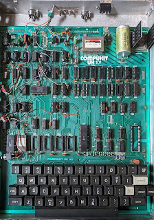
A bodge wire is defined as a "wire added to a PCB to fix errors in the layout or broken traces." The first is as a result of a design fault while the second arises from mistakes made in maintenance of an existing PCB.

Bodge wires don't introduce new functionality, they only restore intended functionality. Therefore they should be as unobtrusive as possible.

When restoring an old computer, bodge wires are frequently necessary to fix traces which have broken due to excessive heat during the desoldering of defective parts for replacement, most often ICs and IC sockets.

Bodge wires

When a trace lifts or breaks, I mark the PCB on the top-side with Tipp-Ex as a reminder that a bodge will be necessary sometime in the future. The bodge is then later made on the bottom-side of the board, to keep things tidy.

Bodges required!

It can be useful to differentiate bodge wires from wires adding functionality by colour, or adding functional wires to the top-side of the board.

Kynar wire, Wire stripper and Magnifier

Essential tools for this are 30 AWG Kynar wire, a Wire Stripper and Eye magnification of some kind. Care is needed to ensure that the correct joints on the bottom-side are actually the correct ones. Check your work with a continuity tester!

Some useful additional tips in the EEVblog.

Tuesday, 9 January 2024

Testing ICs


It seems like about two years ago, IC testers made quite a splash, judging by reviews of the Retro Chip Tester Pro (Adrian's Digital Basement) and the BackBit Chip Tester Pro (Noel's Retro Lab). Nice products though they are, they are a little out of my price range for this project.

TTL testing

Luckily for my wallet, there are several DIY projects out there which can be assembled from commonly-available parts in not too long. Nick Gammon (who's excellent interrupt and power-saving pages were inspiration for my Interrupted project) has a super-simple one which can be assembled on a breadboard in about an hour for the cost of 16 resistors, some dupont connectors and an Arduino Uno!

It ain't pretty but it works!

Nick credits an Instructable by one "JorBi" for inspiration for his work. That project is more elaborate, using an Arduino Nano and a display --- Nick's just uses the Arduino serial port, nothing wrong with that. JorBi's project also provided the data file containing the actual chip tests: JorBi stores this in an EPROM while Nick puts it in the on-chip flash.

Another tester of note is the Smart-IC-Tester: an Arduino shield with TFT display. This stores the test database on an SD card, in a format very similar to JorBi's, just adding a one-line description to each part.

So? Well out of 34 74-series TTL chips on the UK101, Nick's tester flagged 7 as bad, 15 as good, 4 were unknown and 8 not tested, due to having wires soldered to them. Not bad for a day's work!

The bad chips were as follows:

  • Two 74125s
  • Three 74123s (all from the same batch)
  • One 7403
  • One 7404 (in bad shape, one pin broke off in the socket)
Note, it could be that the 74123 and 74125 tests are incorrect. I have none which tested good.

Update: After playing with the IC-Tester for a while longer, I managed to add tests for the hitherto-unknown chips. The latest score is 9 bad, 22 good and 3 not tested. My fork of Nick's repo is here.

Update 2: I built this circuit on a piece of vero board and piggy-backed it onto my home-brew Uno!
An improvement anyway!

Memory testing

In addition to the discrete TTL chips, the UK101 also had 32 2114 static RAM for main memory and another 4 for the display. Nick's tester is unable to test this IC. Luckily somone named "skjerk" has written a sketch for the Arduino Uno which does exactly this.

The 2114 has a pretty bad rep when it comes to living into old age so I didn't hold out much hope for my set. Rather incredibly however they all came up good!

Untested so far

Chips which I haven't been able to test yet:
  • The 6502 and 6851
  • The Basic ROMs and Character Generator ROM
  • The monitor EPROM

Given an EPROM programmer, it should be possible to read the ROMs and compute their checksums. Stay tuned for that!

Of course the two commercial testers mentioned above can test all of these chips, out-of-the-box. But where's the fun in that?

Thursday, 7 December 2023

Desoldering stuff

Progress? Maybe!


Last time, the next planned step was to remove all of the bodges and restore the machine to something resembling a "factory configuration". This aim has changed slightly: a lot of the bodges are gone but some remain:
  • The 48x32 display mod was just too tricky to undo without a display to test it against.
  • Similarly will leave the 300/600 baud and RS-232 mods until a later time.
  • The monitor switch mod also stays until the EPROM has been verified to work.
So what has been done here?
  • The piggybacked RAM and its decoding logic is history. New sockets were added where necessary.
  • The 6522 VIA board is also gone.
  • A new expansion socket was added to facilitate testing with a Logic Analyzer.
To replace the IC sockets I found the following tools essential:
  • Soldering Iron and solder
  • Desoldering pump
  • Headband Magnifier
  • Bench vise
Don't expect existing IC sockets to survive this process! 
  1. Use the desoldering pump to remove most of the solder; this helps free some of the pins but others will probably remain attached. 
  2. Gently lever the socket away from the board: it will likely break, leaving some pins in place. 
  3. Desolder these one by one. 
  4. Some VIAs will most likely remain at least partially full of solder. To clear them, mount the board vertically in the bench vise and heat each VIA from one side while applying the desoldering pump from the other. It may be necessary to fill the VIA with solder before attempting to clear it, counter-intuitive but it works!
  5. When inserting a new socket do not use force. If it doesn't go in easily, repeat step 4 until it does!
To desolder an unsocketed chip:
  1. Use the pump to remove most of the solder as before.
  2. With a small screwdriver gently push each pin until a click is heard. This means the pin is mostly free of solder.
  3. From the other side of the board, gently lever the chip away from the board. If it doesn't move, mount the board vertically as before, heat the pins on the chip side while applying the desoldering pump from the other. Repeat!
This all requires patience, and a steady hand! 

Flux pen, Desoldering braid and Pump

I also ordered a flux pen and desoldering braid which should be as good or better as the desoldering pump. However I wasn't able to get good results with it. Perhaps my soldering iron isn't hot enough?

Adrian's Digital Basement has a great tutorial on this subject. He also has better tools than I do!

Sunday, 22 October 2023

Restoring a UK101


Yes children, computers looked like this once

This contraption is a Compukit UK101 built over 40 years ago by me from a kit. If I remember right, the kit cost £99 (so must have been one of the last ones) and was smuggled across the UK-Ireland customs border in my parents' car.

Its home is a case made out of aluminium by my brother in our school's metalworking shop. Until fairly recently it resided in my father's attic before being rescued in a clear-out.

An unusual feature (by modern standards anyway) was that its manual contained full schematic diagrams. This led to the proliferation of many third-party hardware modifications, in addition to the ones mentioned in the manual itself. I implemented several of the easier ones.

Under the hood.

Under the hood, it is quite a mess! This was a result of inexperience and lack of funds to "do things right". Looking at the board now, the modifications I seem to have made (or at least attempted) are:
  • Switchable Monitor ROMs
  • Double-speed CPU, to 2MHz
  • Double height display, to 64x32 characters
  • Double-speed tape interface, to 600 baud (or maybe even 1200?)
  • RS-232 interface (used to communicate with a Sinclair QL)
  • 8kB RAM expansion, from 1kB (below the UHF modulator and PSU)
  • Extension ROMs 
  • VIA-6522 board (above the keyboard, on the right)
Some time in the 1990s, I pulled all of the ROMs and read them to use as the basis for an emulator which has been described before here. This explains the empty sockets above the keyboard, on the left.

Whether it still works or not is anyone's guess but inspired by Usagi Electric's fine work on a Centurion mini-computer, I've decided it might be an interesting project. A rough outline of the steps involved might be:
  • Verify the power-supply is working. Done!
  • Remove all of the piggy-backed chips and other bodges; replace IC sockets where required; test RAM chips and leave 1kB system RAM and 1kB display RAM.
  • Using a 16-channel logic analyser and the excellent 6502 decoder project, verify that the system boots by comparing the CPU trace to that from the UK101 emulator.
  • Clean up the video circuitry by connecting to a video monitor, either by buying an old one second-hand, or using this adapter to connect to a modern (HDMI) one.
Once all that has been done, I can start to think about adding new hardware:
  • 32kB static RAM chip (62256-80 seems to be suitable) and 16kB ROM (27C128). The former will occupy the lower half of the address space (0000-7FFFh) and the latter the next quarter (8000-BFFFh).
  • Display modifications: double-height, colour.
  • I/O board: disk controller, VIA
One very interesting possibility would be to build a "universal hardware module" out of an Arduino (e.g., an esp32). This would run a modified UK101 emulator and provide all of the missing hardware by listening on the address bus, data bus and CPU control lines. The CPU would initially have no RAM or ROM: it would all be provided by the emulator. (This idea is reminiscent of the ROMulator as featured on Adrian's Digital Basement but would be more flexible.)

Quite a laundry list there: stay tuned!

Thursday, 24 September 2020

Tinysensors Redux


Raspberry Pi Zero-W with Tinysensor Hat

It is often instructive to revisit an old project: you never know what you might see with fresh eyes. Such is the case with Tinysensors, which has featured here several times over the years. Since it lives in Github I use that platform's Issues feature to collect ideas which pop into my head when I am otherwise occupied. This provides a nice context from which to start revisiting.

Among the issues addressed since the last time we featured this project are:

  • Switching to the ATTinyCore. From my point of view, the most important feature of this great project is its support for Optiboot. This decreased the testing time for changes to the Tinysensor sketch by an order of magnitude. No more external programmers!
  • Removing the RF24Network library. This supports a very versatile model of organising nRF24L01+ radios into a fully-connected 5-way tree. However it necessarily limits the number of leaf sensors to 5, requiring bridges to interconnect different levels. A star topology removes this limitation, and also reduces the code footprint enough to support debugging via SoftwareSerial.
  • Reducing power-drain. With the above improvements in testability, it didn't take long before a gotcha in power consumption was spotted: a voltage divider made with a built-in pullup resistor consumes current even during SLEEP_MODE_PWR_DOWN!
  • Moving the hub to Raspberry Pi Zero W. This has more memory and more processor for smaller footprint; in addition to built-in WiFi and Bluetooth. Once that was complete, a proper Hat was designed to hold the nRF24L01+ radio and status LEDs... and a power button, just 'cos.
  • Outsourcing the RF24 library to nRF24. These guys have put a lot of work into improving the performance of Maniacbug's excellent original library, which means I don't have to!
Future work? A nice next step might be to redesign the sensor PCB for a coin-cell and surface-mount components. However I'm pleased enough with these changes to park it for another couple of years!

Thursday, 27 August 2020

Soldering surface-mount components


ncp1402 boost converter


The image shows a breakout board for an NCP1402-based boost converter which steps-up 1.5v to 5v; these circuits are widely-used to power 5v (or nowadays 3.3v) from a single coin cell. (The board is my design, in KiCad, based on the manufacturer's recommended application.)

Of more interest here is the regulator component itself. This is the small 5-pin chip midway up the right-hand side of the board. It is a surface-mount SOT23-5 part, approximately 3mm by 1.5mm, far smaller than a grain of rice. Building this breakout board was more an exercise in seeing if it was possible to hand-solder these parts than anything else, since they are widely available for cheap on t'Internet.

So how did I do it? The first step was choosing a hand-soldered footprint for the part in KiCad. Then, once the boards had arrived, this part obviously had to be soldered on first:

  • Apply solder to the pad under one of the further-apart pins (on the left in the picture)
  • Place the chip over this pad with a tweezers and hold it in place
  • Melt the solder on the pad until it flows over the pin
  • Solder the other pin on the left-hand side
  • Solder the three pins on the right-hand side together
  • With a desoldering pump (braid should work too), remove the excess solder from these three pins, so they are no longer shorted together.
Tweezers and magnifying glass (or low-power microscope) are essential, unless you are some sort of assembly robot. Fine-gauge solder and a fine-tipped soldering are helpful too.

Note that the circuit itself helped me "get away" with the final two steps of the procedure above: of the three pins on that side of the regulator, one is NC and the other two are connected to Vout. However checking with a continuity tester indicated that they were no longer shorted together, so the pump had worked as expected.

So the experiment being successful, the next step is to build more surface-mount parts into my designs. 10k resistors and 100n capacitors crop up very often so they would be obvious targets for replacement. Stay tuned!

Wednesday, 22 July 2020

Simple Variable Voltage Bench PSU

Back in the days of the desktop PC, a common DIY project was to re-use its ATX power supply as the basis of a Bench PSU. Sadly those days are slipping into the past as more and more of us move to laptops. All is not lost however, as most laptop transformers also deliver a reasonable output voltage which can easily be down-regulated and supplied to nascent bench projects.


The circuit schematic could hardly be simpler --- I am fairly embarrassed that the best I could do to obtain it for insertion here was "Print Screen" in KiCad. All of the action is provided by an LM317 linear regulator which costs peanuts these days. The output voltage is given by:

Vout = Vref * (1 + RV1 / R1), Vref = 1.25v

Note that this is independent of the input voltage, although obviously it can't be greater. Also we want to choose R1 so that the output is at sensible values for differing positions of the (linear) potentiometer RV1. Given a transformer rated at 19v, we choose R1 = 680R, giving values of Vout:

RV1    Vout 
0      1.25
2k5    5.8
5k     10.4
7k5    15
10k    19.6

Obviously the last value is a little too high, however this value of R1 gives the greatest precision for the transformer at hand.

The design is completed with a cheap LED voltmeter as shown below.


Simple extensions to this design would be to use a combined Voltmeter/Ammeter display (also costing peanuts); adding a current-limiting circuit, or a switched constant-current source, also supported by the LM317. Next time!