It's relatively easy to test the UK101's discrete TTL chips using a simple Arduino-based IC Tester, and the ROMs can be read by an EPROM programmer but what to do about the more esoteric chips, i.e., the CPU and ACIA?
As CPUs go, the 6502 is a masterpiece of simplicity. It turns out that you can have it run the most basic of programs with no support logic whatsoever! This is the well-known NOP test, in which the CPU is fed an endless stream of No-Operation instructions, see for example here.
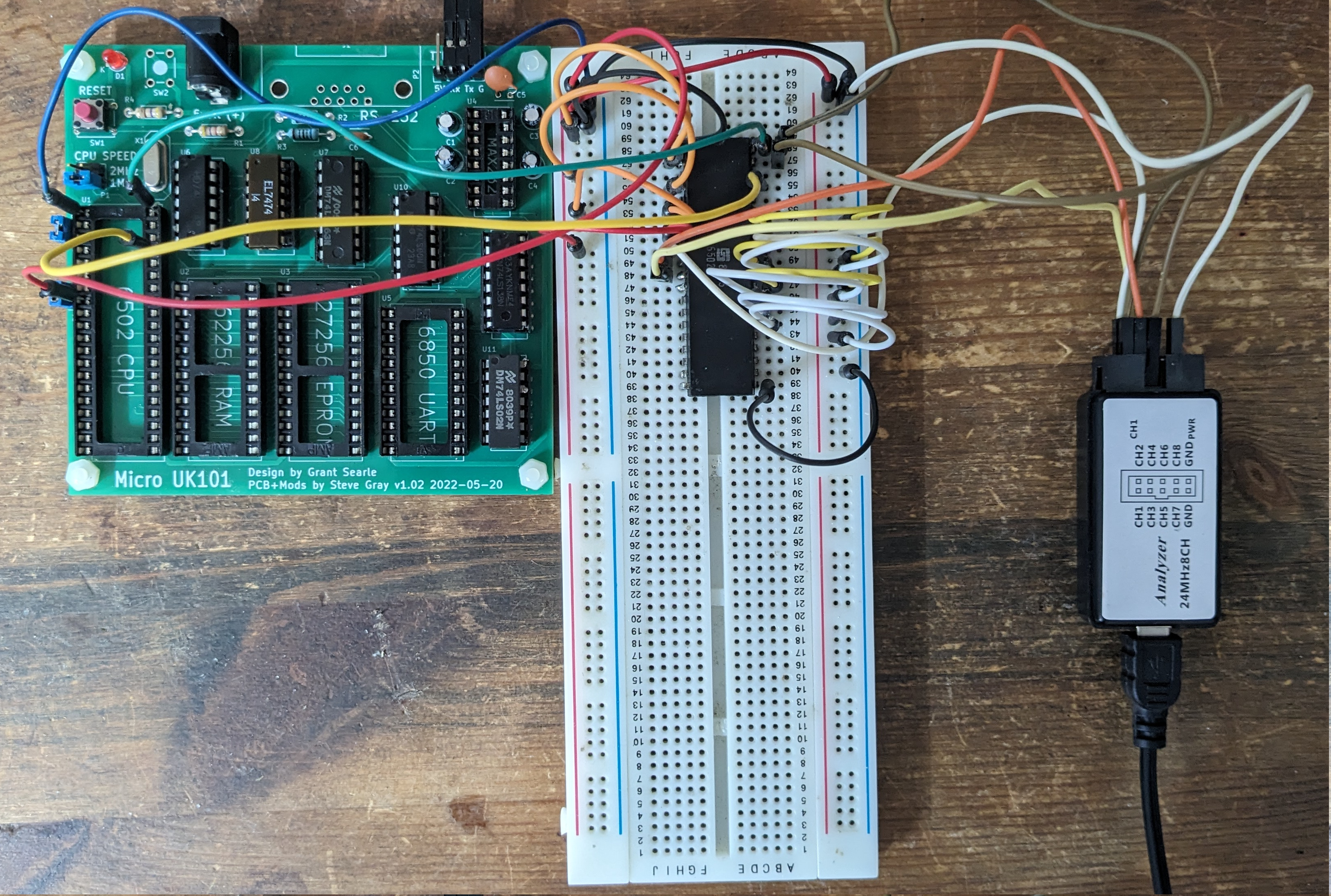 |
| Breadboard 6502 flanked by Clock Circuit (L) and Logic Analyzer (R) |
The image shows the test-set-up. The board on the left is a Micro UK101 which is only used as a power-supply, reset switch and clock source. (This is a more rewarding way of testing CPU and ACIA, but only if they both work!)
The CPU does not need many connections to run the NOP test: its data-bus is hard-wired to EA (the opcode for NOP), it also has IRQ and NMI tied high, and the input clock and reset line from the Micro UK101.
The logic analyser on the right is a cheap 8-channel model which works with PulseView. It is triggered by the reset pin (high-to-low transition) and samples A0, A1, A2 and the output clock.
When powered up and reset, the 6502 reads its reset vector at $FFFC and $FFFD. Unsurprisingly it reads the address $EAEA and jumps there. It then reads an endless stream of NOPs at every address between $0000 and $FFFF. Its address pins will show this.
Or they would show this, if the CPU was working. The screenshot below shows what happens most of the time:
 |
| Dead |
The top trace is the reset line and the bottom one is the output clock, which seems to be working. The three lines in the middle are A0, A1 and A2 with nada.
However sometimes the CPU shows signs of life. About every 10 resets, there would be a short burst of activity for a few microseconds:
 |
| Some signs of life |
So it looks as if this CPU is a goner. It was made by Synertek in the 35th week of 1980 and spent the last 40-odd years in a cold damp attic, where it expired: RIP.
Update: Hans Otten has written about NOP testers here.


